Quantum Transport in Graphene and 2D materials
Realized in only one or a few atomic thicknesses, graphene and 2D materials possess various novel properties that are distinct from those of their parent bulk crystals. Examples include the linear Dirac band in graphene, strong spin-valley locking in semiconducting transition metal dichalcogenides (TMDCs), and topological edge states in 1T'-WTe2 monolayers. In our lab, we take various experimental routes to gain full control over these novel properties, reveal new phenomena and understand the underlying physical processes (see below for the strong electronic interactions effects in suspended graphene bilayers). Different techniques (rotating stage, dual-gates, strain, etc) can be implemented to access different properties and various 2D materials, such as black phosphorus or CrI3, can also be investigated.
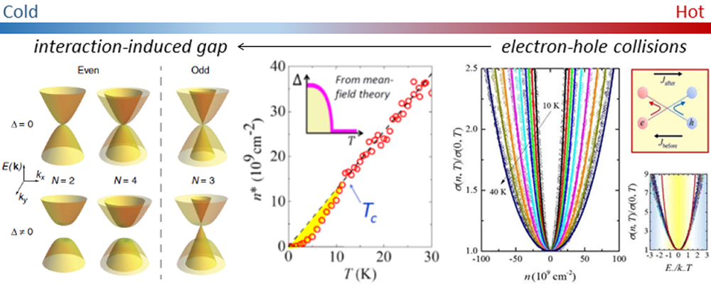
Strong interactions effects in suspended graphene bilayer
Related publications
- Youngwoo Nam, Dong-Keun Ki, David Soler-Delgado, and Alberto F. Morpurgo*, "A family of finite-temperature electronic phase transitions in graphene multilayers", Science 362, 324 (2018).
- Youngwoo Nam, Dong-Keun Ki*, David Soler-Delgado, and Alberto F. Morpurgo*, "Electron-hole collision limited transport in charge-neutral bilayer graphene", Nature Phys. 13, 1207 (2017).
- Lin Wang, Ignacio Gutiérrez-Lezama, Céline Barreteau, Dong-Keun Ki, Enrico Giannini, and Alberto F. Morpurgo*, "Direct observation of long-range field-effect from gate tuning of non-local conductivity", Phys. Rev. Lett. 117, 176601 (2016). *Editors’ Suggestion
- Dong-Keun Ki and Alberto F. Morpurgo*, "Crossover from Coulomb Blockade to Quantum Hall Effect in Suspended Graphene Nanoribbons", Phys. Rev. Lett. 108, 266601 (2012).
'Designer' Electronic Heterostructures and Interfaces
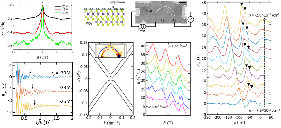
Engineering new electronic properties beyond what Nature provides is one of the central challenges of modern solid-state physics. For this, we design and realize various types of electronic heterostructures and interfaces at an atomic scale, investigate the emergent phenomena and exploit their full potential by understanding the microscopic electronic processes. Examples include hybrids between the materials with distinct properties (e.g., superconductor-magnet hybrids), local-gated lateral or vertical junctions, and van der Waals (vdW) assembled artificial stack of different 2D materials (see below for the vdW-engineered spin-orbit coupling in graphene).
VdW-engineered spin-orbit coupling in graphene
Related publications
- Qing Rao#, Wun-Hao Kang#, Hongxia Xue, Ziqing Ye, Xuemeng Feng, Kenji Watanabe, Takashi Taniguchi, Ning Wang, Ming-Hau Liu*, and Dong-Keun Ki*, "Ballistic transport spectroscopy of spin-orbit-coupled bands in monolayer graphene on WSe2", Nature Commun. 14, 6124 (2023).
- Zhe Wang, Dong-Keun Ki, Diego Mauro, Jun Yong Khoo, Leonid Levitov, and Alberto F. Morpurgo*, "Origin and magnitude of ‘designer’ spin-orbit interaction in graphene on semiconducting transition metal dichalcogenides", Phys. Rev. X 6, 041020 (2016).
- Zhe Wang, Dong-Keun Ki, Hua Chen, Allan H. MacDonald, and Alberto F. Morpurgo*, "Strong interface-induced spin-orbit interaction in graphene on WS2" Nature Commun. 6, 8339 (2015).
- Nuno J. G. Couto, Davide Costanzo, Dong-Keun Ki, Kenji Watanabe, Takashi Taniguchi, Francisco Guinea, and Alberto F. Morpurgo*, "Random strain fluctuations as dominant disorder source for high-quality on-substrate graphene devices", Phys. Rev. X 4, 041019 (2014).
New Topological States of Matter
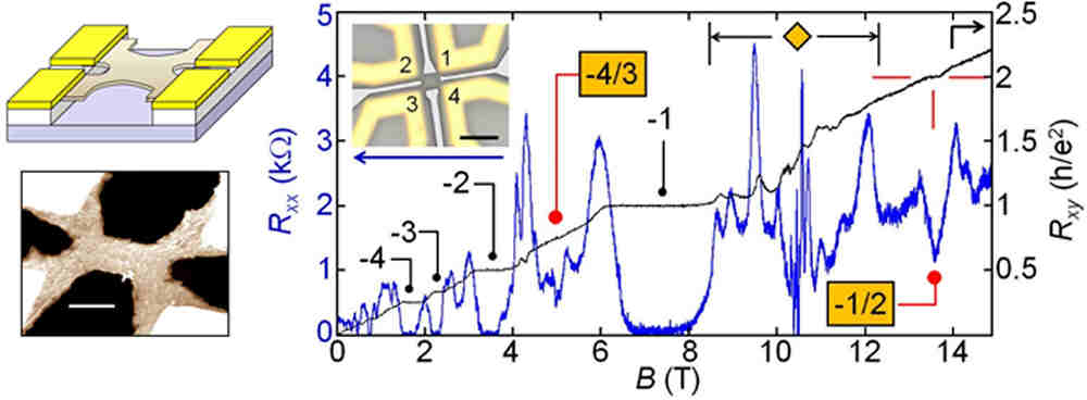
Topological states of matter represent the new class of materials that are characterized by non-trivial topological properties. They can be distinguished from trivial states by the emergence of exotic low-energy quasi-particles at the boundaries, such as Majoranas in topological superconductors and non-Abelian anyons in even-denominator fractional quantum-Hall (FQH) states (see below). In our lab, we aim to exploit full potential of the 2D materials and their interfaces to find or engineer new topological quantum states. Examples include suspended graphene multilayers with superconducting contacts, dual-gated graphene-TMDC or multi-domain vdW heterostructures. We are also interested in exploring various other possibilities that the new materials, such as the recently found 2D magnets, may offer.
Even-denominator FQHE in bilayer graphene
Related publications
- Lin Wang, N. Chepiga, Dong-Keun Ki, L. Li, F. Li, W. Zhu, Y. Kato, Y. Kato, O. S. Ovchinnikova, F. Mila, I. Martin, D. Mandrus, and Alberto F. Morpurgo*, "Controlling the topological sector of magnetic solitons in exfoliated Cr1/3NbS2 crystals", Phys. Rev. Lett. 118, 257203 (2017). *Editors’ Suggestion
- Dong-Keun Ki, Vladimir I. Fal'ko, Dmitry A. Abanin, and Alberto F. Morpurgo*, "Observation of Even Denominator Fractional Quantum Hall Effect in Suspended Bilayer Graphene", Nano Lett. 14, 2135 (2014).
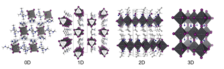
Perovskite Thermoelectrics
Thermoelectric materials generally refer to a group of materials with large thermoelectric effects, i.e., those that have a large figures of merit, ZT = S2σT/κ, where S=-ΔV/ΔT is the Seebeck coefficient, σ and κ is the electrical and thermal conductivity, respectively. They have attracted considerable interests as they can directly convert heat into electricity or vice versa via various phenomena, such as Seebeck effect (generating electricity from a temperature gradient), Peltier effect (adsorbing or evolving heat by flowing an electrical current), and Thomson effect (adsorbing or evolving heat by both an electrical current and temperature gradient). Many efforts have been made to find the materials with larger ZT, i.e., those with a larger Seebeck coefficient, higher electrical conductivity, and lower thermal conductivity, simultaneously, which is difficult as the three parameters are closely related and cannot be tuned independently. Here, we explore various Perovskite nanostructures realized in zero, one, and two dimensions to investigate if they exhibit a large ZT and to find a way to enhance it further using the state-of-art nanofabrication and engineering techniques developed in our group.
Perovskite Nanostructures
Related publications
- Heekwon Lee, Zhuoran Wang, Qing Rao, Sanghyeon Lee, Xiao Huan, Yu Liu, Jihyuk Yang, Mojun Chen, Dong-Keun Ki*, and Jitae Kim*, "Additive Manufacturing of Thermoelectric Microdevices for Four-Dimensional Thermometry", Adv. Mater. 2301704 (2023). *Featured in a frontispiece
- Mojun Chen, Jihyuk Yang, Zhenyu Wang, Zhaoyi Xu, Heekwon Lee, Hyeonseok Lee, Zhiwen Zhou, Shien-Ping Feng, Sanghyeon Lee, Jaeyeon Pyo, Seung Kwon Seol, Dong-Keun Ki, and Ji Tae Kim*, "3D Nanoprinting of Perovskites", Adv. Mater. 31, 1904073 (2019). *Featured in a front cover
- Seung-Geol Nam, Dong-Keun Ki, and Hu-Jong Lee*, "Thermoelectric transport of massive Dirac fermions in bilayer graphene", Phys. Rev. B 82, 245416 (2010).