-
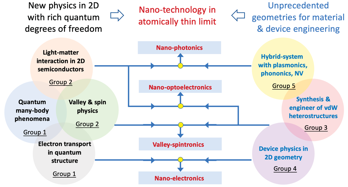
Two-dimensional (2D) materials have a great potential for microelectronics and information technology. The variety of 2D materials feature a wide range of material properties from metal, semiconductors, insulators to magnets and superconductors, as well as exotic physics associated with electrons' quantum degrees of freedom (e.g. spin and valley) that could be exploited to encode and process information efficiently. Their tiny thickness - just a few atoms - promises the ultimate miniaturization of devices, and unparalleled control of materials and device functions. Moreover, 2D materials feature an unprecedented flexibility in their assembly into heterostructures, through which new materials and device functionalities may emerge. This project brings together leading physicists, engineers, and chemists on 2D materials research, to explore new opportunities and tackle grand challenges in a number of areas from fundamental science to technological applications in electronics, optoelectronics and photonics. The topics and interactions of this interdisciplinary project are illustrated below.
-
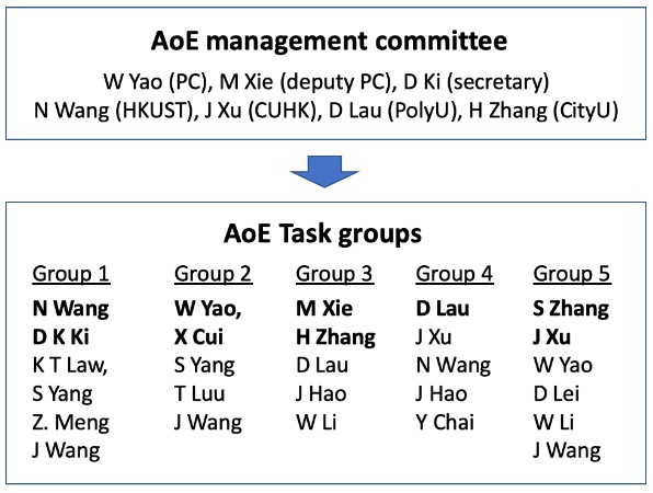
Our research team members are divided into five interconnected Task Groups to work on the seven themes. These Task Groups are organized according to our objectives as well as the expertise of the members. They form an overall coherent research program.
-
Mission
-
To explore fundamental physics in the new realm of two-dimensional atomic crystals and their van der Waals heterostructures with the abundant quantum degrees of freedom (e.g. spin, valley); and to explore quantum engineering of materials and devices in the unprecedented atomically thin 2D geometries, with the aim to revolutionize electronics, optoelectronics and photonics.
-
Goals
-
To explore the physics of spin & valley in 2D materials, and new mechanisms of device operations and information processing based on control of these quantum degrees of freedom.
To explore electron transport, and light-matter interaction in quantum structures of 2D atomic crystal, and exploit their full potentials for new electronic and optoelectronic applications.
To explore superconductivity, and new quantum states of matters in 2D materials and their moiré superlattice.
To develop growth methods so as to synthesize new 2D materials, to improve materials qualities, towards large-scale wafer-size growth, and to engineer various van der Waals heterostructures.
To investigate the fabrication and engineering of devices under the new geometries enabled in the ultimate 2D limit, and the device physics in the atomically-thin heterostructures.
To explore hybrid systems of 2D crystals with plasmonic structures, metamaterials, phononic systems, defects in nano-diamond, for expanding their scientific & technological applications.