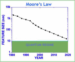
Decrease of feature size has been the driving force in electronics. With smaller sizes, there are more transistors on a chip, allowing higher speed and larger memory in computers, cell phones, IPODs, and other consumer electronics.
We strive to develop a suite of multi-scale electronic design automation (EDA) tools ranging from atomistic simulation methods to circuit simulators and to electromagnetic solvers for electrical signals for emerging sub-22nm technology. With these tools, we will study the sub-22nm devices and their systems; and calculate their physical and dynamical properties, and explore the possible paradigm shifts of next generation electronics. Our objectives are specifically listed below:
-
To simulate from first-principles the electrical properties and processes of sub-22nm devices with atomistic details
-
To investigate lithography modeling, and to employ efficient electromagnetic solvers to simulate electrical signals, power delivery, crosstalk, interference, and noise in multi-scale complex integrated circuits
-
To calculate and model the electrical, chemical and mechanical properties of new materials for sub-22nm technology
-
To develop modeling tools for the emerging spintronics and magnetic random access memory (MRAM)
-
To use electron beam lithography technology to fabricate the sub-22nm devices for measurement and calibration of the parameters in our EDA tools
-
To develop a set of multi-scale EDA tools for emerging devices and integrated circuits
-
Our former students and postdoctoral fellows are working in leading IT companies (such as Intel, IBM, HP, Cadence, Agilent, Qualcom, Synopsys, TSMC and SMIC)
-
Members have received funding from leading IT companies including SRC, IBM, Intel, and Mentor Graphics
-
Five Innovation and Technology Funds have been awarded to our team members
-
Several computer clusters including a 64-bit Linux cluster (consisting of 16 blade servers; each equipped with two 64-bit six-core Intel Xeon CPU running at 3GHz and 48GB physical memory, and theoretically delivers the processing power up to 2.304 Tera-flops)
-
Multi-chamber ultrahigh vacuum (UHV) system with a UHV-scanning tunneling microscope (STM) and atomic force microscope (AFM), low energy electron diffraction (LEED), reflection high-energy electron diffraction (RHEED), and X-ray photoelectron spectroscopy (XPS)
-
Confocal microscope based spectroscopy system, a femtosecond laser system, and an electrical probe station
-
Low temperature (He-3 cryostat) and high magnetic field transport measurement platform
-
Nanofabrication Fabrication Facility (NFF), in HKUST, is the first micro and nanofabrication laboratory established at a tertiary institution in Hong Kong. The mission of the NFF is to provide facilities for the faculty and students of all the UGC funded institutions to conduct teaching and research, particularly in new semiconductor devices and nanoelectronics process technology
-
Material Characterization and Preparation Facility (MCPF), in HKUST, is a central facility intensively serving the academic researchers and postgraduate students in schools of science and engineering for the preparation, characterization and analysis of various advanced materials. In addition to serving HKUST, MCPF also provides services to Hong Kong sister institutions and clients from government laboratories and regional industries. Since the MCPF was established in 1991, it has become an indispensable central facility in HKUST
Post-doctoral Fellows and Research Assistant Professors for the Area of Excellence Project
Post-doctoral Fellows and Research Assistant Professors for the Area of Excellence Project (Ref.: 201501334)
Applications are invited for appointments as Post-doctoral Fellows (PDFs) and Research Assistant Professors (RAPs) in Emerging Electronics for the AoE Project, to commence as soon as possible for one to three years, with the possibility of renewal.
Applicants should possess a doctoral degree in Physics, Chemistry or Electrical Engineering, with strong experience in Computational Science and Engineering. Successful candidates will join a multi-institutional interdisciplinary project on modeling and simulation of emerging electronics in Hong Kong to develop a suite of multi-scale electronic devices and automation software tools. Details can be found at http://www.physics.hku.hk/AoE_Electronics/ .
PDFs are expected to devote full-time to research. Applicants should be doctoral degree holders having undertaken original research that has contributed to the body of knowledge.
For RAPs, the main focus of their duty is research. They can however be assigned some teaching duties, up to 50% of the normal teaching load. Applicants should be research active and have a proven publication record.
Applicants who have responded to the previous advertisement (Ref.: 201400300) need not re-apply.
A highly competitive salary commensurate with qualifications and experience will be offered, in addition to annual leave and medical benefits. The appointments of RAPs for two years or more will attract a contract-end gratuity and University contribution to a retirement benefits scheme, totalling up to 15% of basic salary.
Applicants should send a completed application form, together with an up-to-date C.V. and a cover letter by e-mail to physdept@hku.hk . Please indicate clearly the reference number and which position they are applying for in the subject of the e-mail. Application forms (341/1111) can be downloaded at http://www.hku.hk/apptunit/form-ext.doc . Further particulars can be obtained at http://jobs.hku.hk/.Closes February 28, 2016.
The University thanks applicants for their interest, but advises that only candidates shortlisted for interviews will be notified of the application result.