We are an experimental research group on solid state physics at Physics department, University of Hong Kong.
Our research focuses on characterizing optical and electric properties of materials at micro and nanoscales. The current efforts concentrate on optical properties of two-dimensional semiconductors with optical spectroscopic techniques.
2D semiconductors
Our research focuses on characterizing optical and electric properties of materials at micro and nanoscales. The current efforts concentrate on optical properties of two-dimensional semiconductors with optical spectroscopic techniques.
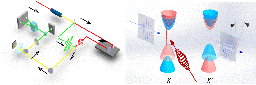
With the spatial dimensions reducing from 3D to 2D, there are some significant changes in characteristics. First, the Coulomb interaction is tremendously enhanced due to the spatial confinement and weak Coulomb screening. This leads to giant exciton binding energy robust enough at ambient temperature and lowers the threshold for many-body effects and quantum phase transitions. Second, the spatial confinement to 2D renders energy dispersion and 2D momentum space. For example, the density of states in 2D is a linear function of effective mass only instead of a dispersion of energy in 3D. These differences could lead to different phenomena in 2D system. The conventional 2D system is constructed at the interface of heterostructured semiconductors. Nowadays tremendous interests on 2D semiconductors concentrate on the atomically thin 2D crystals (for example, bi/multilayer graphene, transition metal dichalcogenides, monochalcogenides). We have been exploring the exciton physics, spin and valley quantum states in atomically thin 2D semiconductors particularly monolayer/multilayer transition metal dichalcogenides (MoS2, MoSe2,WS2, WSe2). We are investigating the interactions of exciton-exciton, exciton-electron, electron-electrons, etc and the interplay of orbits, spin, valley degrees of freedom in 2D. The research tools involved are semiconductor micro-optics techniques and the home-built setup covers a wide range of techniques from photoluminescence, Raman, reflection, Kerr rotation to ultrafast pump-probe spectroscopy.
Apparatus Development
Research equipment development is a hobby for experimentalists in solid state physics. So do we. We are interested in experimental setup development and apparatus DIY. The on-going hobby project is an energy resolved X-ray semiconductor detector, going slowly though.