Yao Group @ HKU Physics
|
Valleytronics in 2D materials and their moire superlattices A trend in future electronics is to utilize internal degrees of freedom of electron, in addition to its charge, for nonvolatile information processing. Suitable candidates include the electron spin, and the valley pseudospin. The latter labels the degenerate valleys of energy bands well separated in momentum space. 2D materials, in particular the semiconducting transition metal dichalcogenides, offer an exciting platform to explore valleytronics and spintronics. Moiré pattern is the superlattice structure created when 2D materials are stacked with crystallographic misalignment resulting in spatial variation in the interlayer atomic registries. Because of the inevitable mismatch in lattice constants of different 2D materials and twisting between their crystalline axes, moiré pattern can be generally present in van der Waals layered structures. The creation of long-wavelength moiré pattern is becoming a powerful approach to engineer the electronic and optical properties of vdW structures of 2D materials. We have discovered a varieties of valley and spin phenomena that make possible their manipulations in the 2D materials and their moire superlattices. |
|
|---|---|
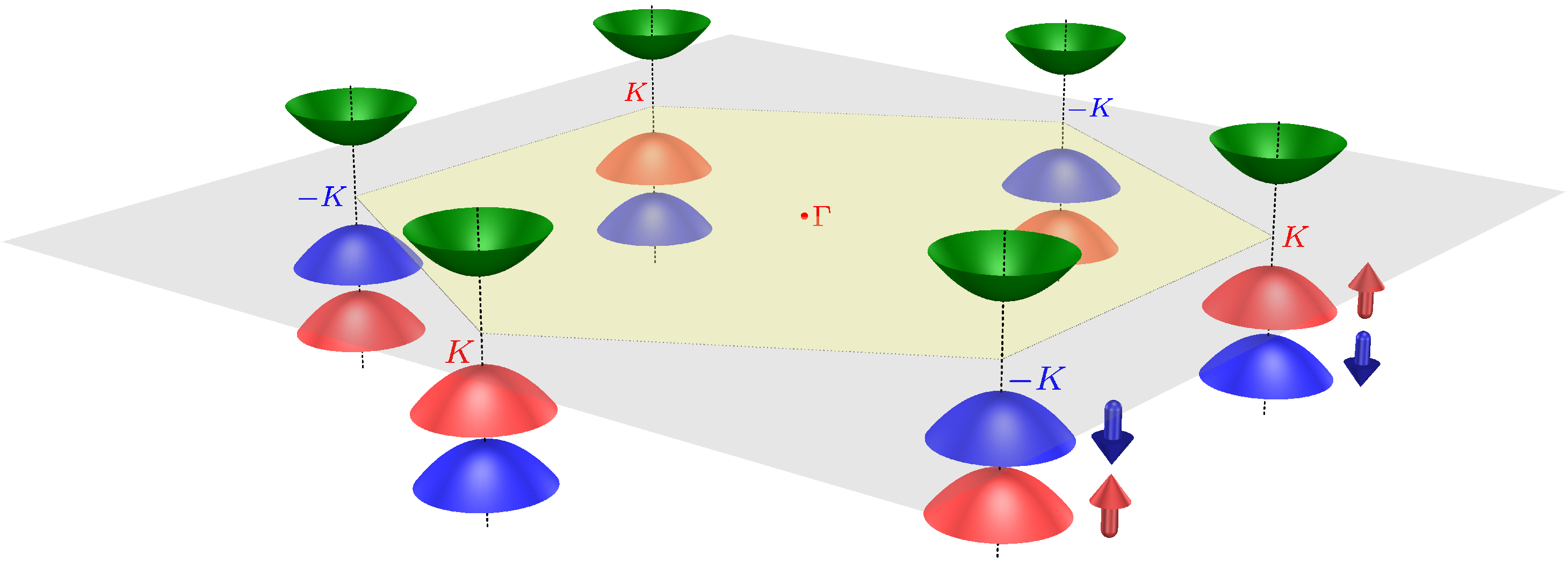
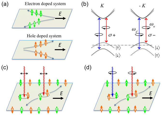
[Top] Schematic drawing of the band edges in semiconducting transition metal dichalcogenides monolayers. Spin-orbit coupling leads to an effective locking of spin and valley indices. [Right] Spin-valley coupled physics in monolayer transition metal dichalcogenides. The electrons and holes in valley K are denoted by white ‘-’, ‘+’ symbol in dark circles and their counterparts in valley -K are denoted by inverse color. (a) Valley and spin Hall effects in electron and hole doped systems. (b) Valley and spin optical transition selection rules. Solid (dashed) curves denote bands with spin down (up) quantized along the out-of-plane direction. (c) Spin and valley Hall effects of electrons and holes excited by linearly polarized optical field. (d) Spin and valley Hall effects of electrons and holes excited by two-color optical fields. From Xiao, Liu, Feng, Xu & Yao, Phys. Rev. Lett. 108, 196802 (2012). — (Link) |
|
|
Reviews and book chapters |
|
|
Valleytronics in 2D materials, J. Schaibley, H. Yu, G. Clark, P. Rivera, J. Ross, K. Seyler, W. Yao and X. Xu, Nature Reviews Materials 1, 16055 (2016). — (Link) |
|
|
Valley excitons in two-dimensional semiconductors, H. Yu, X. Cui, X. Xu and W. Yao, Natl. Sci. Rev. 2, 57 (2015). — (Link) |
|
|
Electronic structures and theoretical modelling of two-dimensional group-VIB transition metal dichalcogenides, G. Liu, D. Xiao, Y. Yao, X. Xu and W. Yao*, Chem. Soc. Rev. 44, 2643 (2015) — (Link) |
|
|
Spins and pseudospins in layered transition metal dichalcogenides, X. Xu*, W. Yao*, D. Xiao and T. F. Heinz, Nature Physics 10, 343 (2014). — (Link) |
|
|
Valley-Spin Physics in 2D Semiconducting Transition Metal Dichalcogenides, H. Yu and W. Yao, In P. Avrouris, T. Heinz & T. Low (Ed.), 2D Materials: Properties and Devices, Cambridge Univ. Press. (2017) — (Link) |
|
|
Optical Properties of TMD Heterostructures, P. Rivera, W. Yao and X. Xu In P. Avrouris, T. Heinz & T. Low (Ed.), 2D Materials: Properties and Devices, Cambridge Univ. Press. (2017) — (Link) |
|
|
Interlayer valley excitons in heterobilayers of transition metal dichalcogenides, P. Rivera, H. Yu, K. Seyler, N. Wilson, W. Yao, X. Xu, Nature Nano. (2018), Advance online publication |
|
|
Valley excitons: From monolayer semiconductors to moiré superlattices, H. Yu, X. Xu, W. Yao, In Steven T. Cundiff & Mackillo Kira (Ed.), Semiconductor Quantum Science and Technology, Elsevier. (2020) — (Link) |
|
|
Quantum Spintronics We are interested in the quantum coherent control of spins in solid state systems, including the electron spins localized in semiconductor nanostructures and the lattice nuclear spins. |
|
| Quantum decoherence in a nuclear spin bath | |
| Optical quantum control of localized electron spin in semiconductors | |
| Manipulation of spin ensemble via collective channels | |
|
|
|